Efficient, simultaneous testing of thousands μLEDs on a wafer or in modules within a few seconds
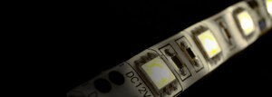
MicroLEDs are renowned for being an exacting new display technology. They are smaller than 100 micrometers and have exceptional optical properties that enable the manufacture of displays with a wide color gamut, high contrast and extremely high resolution. Also new adaptive front-lighting systems (AFS) for automotive use MicroLED arrays with several 10,000 individual light sources. This enables precise control of the light beam, as each MicroLED can be controlled individually.
The challenge in MicroLED in-process inspection
µLED wafer & display probing
Particularly in production, millions of μLEDs on a wafer or display present new challenges for the optical quality tests:
- Parallel testing of thousands or millions of μLEDs
- Simultaneous electric probing or optical excitation of as many μLEDs on a wafer as possible
- Fast and accurate optical inspection on every LED or pixel, synchronized with production flow
- Color & luminance homogeneity
- Dominant and peak wavelength
- Spatial resolution - Camera system calibrated with full traceability to national labs
- Adaptive calibration for spectrally variant light sources
µLED arrays for automotive adaptive front lighting systems
Ultra-bright high-performance LED modules can be challenging:
- Variant spectral properties of the underlying semiconductor and phosphor
- Temporal synchronization to light source driver
- Spatial resolution
- Cross talk
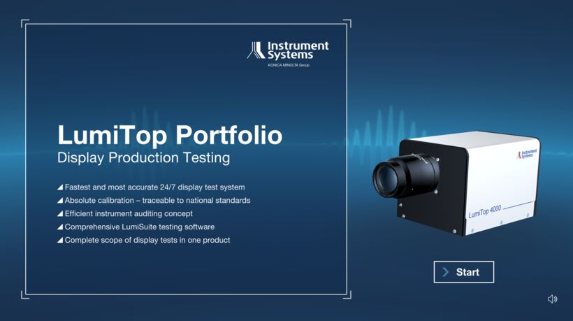
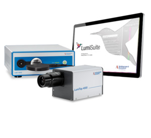
Our solution: Camera-based LumiTop 2D system
With the camera-based LumiTop 4000 and LumiTop X150 2D system, Instrument Systems provides fast, highly accurate and traceable optical measurements of different μLED arrays and display probes. The combination of our high-accuracy CAS 140D spectroradiometer and different LumiTop cameras allows a live adaptive calibration based on the spectral properties of the device under test.
In addition, the measurement can be synchronized to the current source of the μLED for speed and high reproducibility. Compared to measuring each LED of the wafer individually, the simultaneously measuring LumiTop system is orders of magnitude faster and still provides spatial and spectral information for every individual emitter. Instrument Systems is a test laboratory accredited to ISO 17025 and guarantees traceable measured values with known accuracy.
The LumiTop 4000 has a resolution of 12 MP and can detect the smallest of defects and inhomogeneities. With a 100 mm macro lens, the camera enables fast parallel inline analysis of all μLEDs on a wafer at a single test station. With a field of view (FOV) of approx. 10 by 14 mm it can measure many thousands of μLEDs in parallel with a minimum pixel size as low as 30 micrometers.
LumiTop X150 features a 150 MP sensor with up to 600 MP by optional pixel shifting. Various lens options adapt to the device under test (DUT) from microdisplays and wafers to large video walls. With LumiTop X150 even one-shot wafer tests become possible.
Both LumiTop systems allow customized calibration options to optimize accuracy specifically for µLED applications.
We will be pleased to provide advice for your planning in order to configure the ideal measuring concept.
What is your individual challenge? Together we can find the right solution – just ask us!
Video: Learn more about our MicroLED measurement solutions